Today i made my first pcb at home, we use to make PCB at college lab, there they used photoresist method which was very tedious and also because of having lots of students we were unable to make as much as i want...!!
So after searching a lot on net and finding here and there, so today i tried to make PCB at home only. So lets get started...
I will classify this process in 4 steps..
1) Making PCB design, using any CAD software
2) Transferring it to Copper clad
3) Etching
4) Placing Components
Lets proceed step by step.
1) Making PCB design, using any CAD software
Download any free PCB designing software, FreePCb, Express PCB, PCB wizard. I used PCb wizard because its very easy to work upon with, but the major problem is that it doesnot has large library for components, so only useful when you work with basic components. Any way get back..
Place the components and draw the circuit.
You can refer to my tutorial on using PCB wizard
You can download the software here
FREE PCB http://www.freepcb.com/
PCB WIZARD http://www.4shared.com/file/1sWVfT-i/PCB_Wizard_350_Pro_Unlimited.htm?aff=7637829
for example here in this tutorial we will make PCB for my ir_sensor_for obstacle avoidance
you can refer to my tutorial on making IR_SENSORS


2) Transferring it to Copper clad
Take the print out of the design in a "GLOSSY PAPER",(which is used to print photos), through LASER PRINTER (i have used Samsung's ML 1610 ) which looks like this

(note: this is print of a different circuit)
Requirements for this step
1) HEATING IRON
2) COPPER CLAD BOARD
3) DESIGN PRINTED ON GLOSSY PAPER
Cut the copper clad board in required dimension according to the circuit,

as the copper clad is covered by oxide layer, clean the surface using dish cleaner pad using any of the utensil cleaning liquid(i used VIM liquid)


till it gets shiny in appearance and let the surface dry for few a minute

never touch again the top surface with fingers because the oil from hands gets on the board which affects the development process,
First heat the copper plate, for this place a normal white sheet on copper plate and then apply heated iron for 30 seconds,

remove the paper and then place the design on copper plate(Glossy/design side down on copper side)

and then press the heated iron for near about 6-7 minutes, the design will get stick to the plate completely, lift the iron and press the edge portion also nicely..
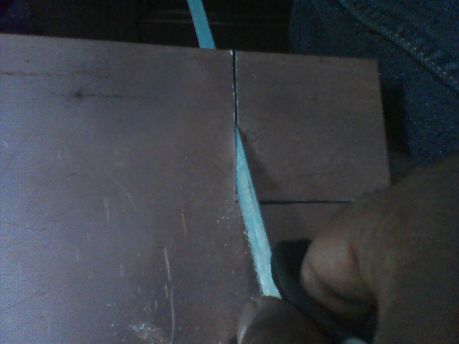
Soak the plate+paper combination in normal water for about 5 minutes after that start removing the paper by rubbing it, use brush(ex tooth brush ;) ) to remove tiny bits of paper in between the tracks.


if there is any break in track, use permanent marker and complete the track.
3) Etching
Make ferric chloride solution using anhydrous fecl3(in solid form in brownish color) which is available in any online robotics shop nowadays or any local hardware shop,

Solution can be made of any desired concentration, as an idea i used 110 gm of anhydrous ferric chloride to 300ml of water.
To make this first take precautions, read necessary security measures, use gloves and make always make solution in open space with ventilations ,take water in "NON metallic" container ex: tupperware and then add fecl3 to it. DONOT TOUCH FECL3 WITH BARE HANDS (ex use plastic spoon) DONOT INHALE THE GAS COMING OUT OF THE MIXTURE

Tie a string to pcb on back side and then dip it in solution and keep moving it to and fro; within 5 minutes copper starts coming out , keep doing it until the cicuit becomes clear, DONOT LEAVE THE WHOLE CIRCUIT IN SOLUTION FOR HOURS..!! it will dissolve the whole ciruit
Clean the PCB thorougly with water without touching it.And the result would look like this

Store the used ferric chloride solution in a plastic or glass jar for reuse next time,

You will notice as the time and number of circuits etched by the same solution the "etching strength" of it goes on decreasing, means now it will take more time to etch the pcb , to rejuvinate its strength, when you use solution next time add small amount of HCL to it and put the container of fecl3 solution surrounded by warm water, in a bigger plastic container.
4) Placing Components
Drill the holes in the PCB, you can refer to my tutorial on how to make HOME MADE PCB DRILL


Place the components and solder it to the tracks and its done...!!!


And you know what.., it works also.. :P

There are lots of good videos on youtube showing this method, this is a good one..
Bhai ektarfaa....
ReplyDeleteGood Piyu.....
ReplyDelete:) Thanks Mandal sir
DeleteReally helpful.......and I like the way things are explained here...
ReplyDelete:)
DeleteGreat job done!Thanks for taking time to share your creative work,Its been really helpful for the newbies..
ReplyDelete:) Its always like that, we all learn from each other//
DeleteHi, I’ve been a lurker around your blog for a few months. I love this article and your entire site! Looking forward to reading more
ReplyDelete